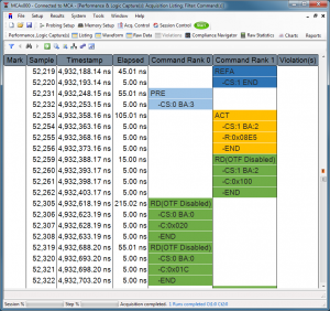
 Logic Validation – (State/Cycle analysis viewing multiple signals as Commands and Data)
The analog characteristics have been validated and it’s time to move on to cycle based analysis. Visibility of commands such as Read and Write with their associated data is acquired and analyzed for accurate bus transactions. A Logic Analyzer or Memory Compliance Analyzer is typically used to acquire dozens or hundreds of signals and software is provided that displays the acquired signals as commands and data. You can see if the target is running as expected. Are commands and data accurate or is there an issue with the command transfer on the bus?
Oversampling of the bus is available and provides insight into the timing of the signals that form the command/data so you can see in a timing display if there are timing issues with signals relative to the system clock (or strobes for data) that is resulting in bad command or data transactions.
Requirements for Logic Validation include:
- Deep trace buffers where hundreds of million or a billion cycles can be acquired for analysis.
- Easy graphical setup of the sample points so each signal can be acquired relative to the clock and with individual voltage/threshold settings.
- Extensive triggering at target speed for focused acquisition.
- Interposers that break out the signals to a Logic Analyzer or Memory Compliance Analyzer for easy and accurate analysis.
As with Electrical Validation, Logic Validation faces similar interconnect/interposer challenges. However, for logic validation you must access all signals on the slot or memory component that are required for Command/Data analysis.
DIMM/SODIMM/Mini-DIMM Analysis
For traditional DIMM/SODIMM/Mini-DIMM configurations it is an electrical challenge to snoop the bus with interposers. Years of development knowledge is designed into every slot interposer developed providing unintrusive high fidelity analysis capability that is easy to install onto a target.
Memory Components (DDR4/LPDDR3/4, PoP, etc)
Memory components with ever shrinking package pitches and Package on Package (PoP) that places the memory component on top of the SOC, present an electrical AND mechanical challenge for interposer development. Gaining access to the signals is a major hurdle that must be overcome. High fidelity interposers that break out the signals at the memory component must:
- Mechanically fit in the target space.
- Maintain the signal fidelity on the target.
- Present an accurate representation of the signal to the test equipment for analysis.
- Reduce probing complexity.
- Provide models for simulation.
Interposer designs are created implementing the years of knowledge gained that started with our first memory interposer. We now achieve accurate analysis that exceed the maximum rates of current technologies such as LPDDR4 at 4.266 GHz. The designs are verified with extensive simulation and unique layout and fabrication techniques to produce industry leading solutions. Enabling the market with an interposer is part of the challenge. The other is providing an easy/unique install capability and access to probing with your Logic Analyzer or Memory Compliance Analyzer.
The installation of the component interposer can be a direct solder of the interposer to your target if you have mechanical clearance. If you do not, sockets the same size as the memory component are assembled onto your target. The socket installation is the same process used to put the memory component onto your target. Once installed the interposer is then press fit onto the socket. When your analysis is completed, you can remove the interposer and install a memory component directly onto the socket.