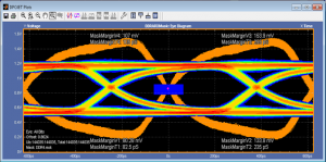
 Product analysis and validation starts by examining the analog characteristics of the signals on your memory bus using an oscilloscope. Signal integrity, Jitter and Drift are looked at and augmented with compliance software used on the oscilloscope that automates the memory compliance verification. However, as clock rates increase and memory components shrink with smaller pitches and Package on Package (PoP) that places the memory component on top of the SOC, gaining access to the signals is a major hurdle that must be overcome. High fidelity interposers that break out the signals at the memory component must:
- Mechanically fit in the target space.
- Maintain the signal fidelity on the target.
- Present an accurate representation of the signal to the test equipment for analysis.
- Reduce probing complexity.
- Provide models for simulation and de-embedding.
Interposer designs are created implementing the years of knowledge gained that started with our first memory interposer. We now achieve accurate analysis that exceed the maximum rates of current technologies such as LPDDR4 at 4.266 GHz. The designs are verified with extensive simulation and unique layout and fabrication techniques to produce industry leading solutions. Enabling the market with an interposer is part of the challenge. The other is providing an easy/unique install capability and access to probing with your oscilloscope.
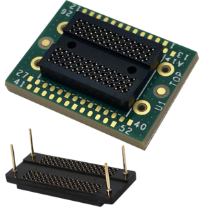
The installation of the interposer can be a direct solder of the interposer to your target if you have mechanical clearance. If you do not, sockets the same size as the memory component are assembled onto your target. The socket installation is the same process used to put the memory component onto your target. Once installed the interposer is then press fit onto the socket. When your analysis is completed, you can remove the interposer and install a memory component directly onto the socket.
Probe points on the interposer for oscilloscope probe tip placement increase the size of the interposer sometimes making it too large for an application. Nexus patented edge probe design places the probe points on the edge of the interposer reducing the physical size of the interposer while providing convenient, easy to access probe points.
Of course, simulation models must be available and are used to simulate the interposer in your target and also for the creation of oscilloscope de-embedding filters. All interposers include simulation models.
XH Series
Nexus Technology’s XH Series interposers bring new enhancements to the EdgeProbe™ and Direct Attach types of memory component interposers that maintain signal integrity across the interposer path as well as provide for extremely high-fidelity oscilloscope probe points for both leading edge and emerging memory technologies such as DDR5, LPDDR5, DDR4 and LPDDR4.
EdgeProbe™ Interposers
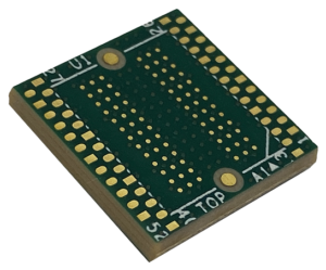
Nexus’ patented EdgeProbe™ designs require a small mechanical footprint by designing the probe points on the edge of the interposer. They are attached directly to the target. Since the number of signals that can be probes is limited to the edge space available some edge probes have a subset of the signals available. When this happens Nexus typically makes more than one version of the interposer. The typical solution would be one interposer that provides access to the CLK and Command bus and all Address signals and a sample of the Data and Strobes or access to the CLK and Command bus and all Data and Strobe signals and a sample of the address.
Socketed Interposers

Typically provides access to all component signals and elevates the interposer above adjacent components for mechanical clearance. This solution offers a custom socket that is installed on the target and has an interposer that is installed by pressing it onto the socket. Retention is designed into the solution since the interposer can be removed by pulling an unsecured interposer from the target socket. The interposer can have the memory component soldered directly to it or optionally have a socket on the interposer. The socket on the interposer allows for memory components to be press fit and removed if you want to easily evaluate different vendor memory components. When testing is completed, the interposer can be removed and the memory press fit directly into the custom socket on the target essentially removing the affect of the interposer in the target.
Logic and Compliance testing (logic analyzer and command protocol) can typically be done by swapping the electrical interposer with an interposer designed for a logic analyzer or Nexus Compliance analyzer for quick and easy analysis.
Direct Attach Interposers

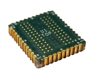
This is an interposer that typically enables probing of all signals and is installed directly onto the target. The target must have mechanical clearance for the interposer. Package on Package (PoP) components have an inherent elevation and the use of the direct attach interposers is common for this application.
